Semiconductor manufacturing: mastering every stage with UHP solutions

1. Gas Delivery to Semiconductor Fabrication Facilities
Ultra-high-purity (UHP) gases are typically delivered to semiconductor fabrication facilities (fabs) through bulk gas systems that handle large volumes necessary for continuous operations. Initially, gases are sourced from high-volume support systems and then routed into the fab via meticulously maintained piping networks. Gases undergo rigorous purification processes and are carefully regulated to maintain purity, pressure, and consistency. Leak-tight integrity of gas handling systems is critical at every stage to ensure safety, prevent contamination, and sustain optimal manufacturing conditions.
Our key solutions for gas delivery:
- UHP bellows valves and diaphragm valves for transportation through tube trailers
- UHP bellows valves for bulk gas initial entry into fabs
- Diaphragm and tied-diaphragm cylinder valves for precision control and purity assurance
- UHP gas Pressure regulators for maintaining consistent pressure and flow
- Vacuum generators ensuring contamination-free
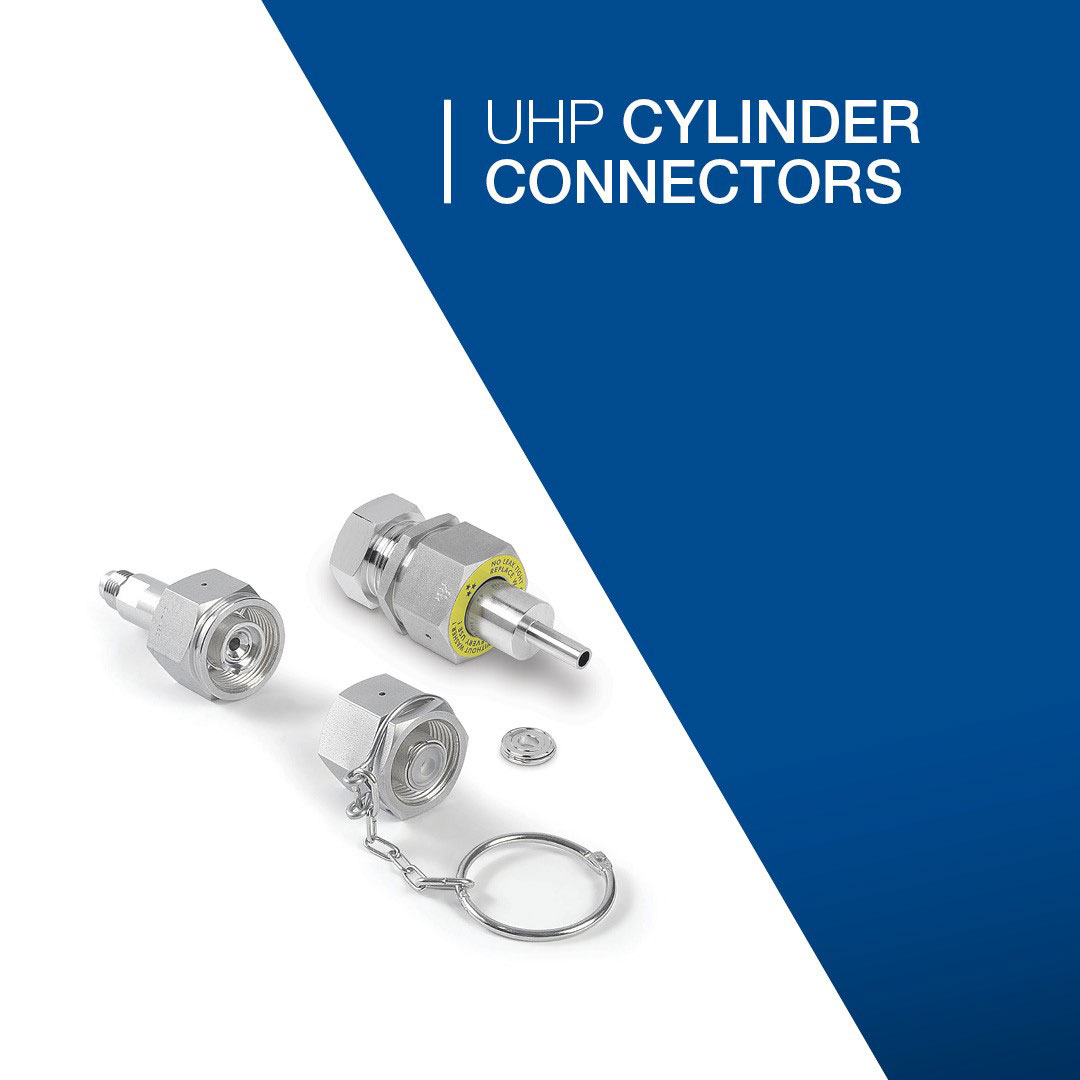
- High-quality fittings to maintain leak-tight integrity and gas purity.
2. Oxidation
Thermal oxidation is typically one of the first steps, forming a layer of silicon dioxide on the wafer surface (e.g. for gate oxides or isolation layers). This is done by heating silicon wafers to high temperature in an oxidizing atmosphere of ultra-high-purity oxygen or water vapor.
The silicon wafer is heated to high temperatures (up to 1100°C) in an atmosphere of UHP O₂ or water vapor to form a thin layer of SiO₂. This layer serves as an electrical insulator for transistors. In wet oxidation, UHP H₂ is combined with O₂ to generate pure vapor. The uniformity and purity of this layer are critical.
Our key solutions for oxidation:
- Diaphragm-sealed valves to precisely manage UHP oxygen (O₂), hydrogen (H₂), and HCl gases in oxidation furnaces.
- UHP gas regulators maintaining stable and consistent gas pressures throughout the oxidation process.
- UHP fittings and connections to preserve gas purity, integrity, and ensure leak-tight operation.
3. Photosensitive resin deposition (Coating)
Before lithography, a photoresist (light-sensitive polymer) layer is applied to the wafer. In this coating step, a photosensitive liquid is applied by spinning to create a uniform film on the wafer. This film will enable pattern transfer during UV exposure. Any variation in thickness or contamination will result in critical defects.
The coating process itself is primarily a liquid/solid application, so it doesn’t involve reactive gases like some other steps. However, UHP nitrogen (N₂) is widely used during resist coating for several reasons. It's important to note that there are two types of photoresist solutions: negative and positive. Positive resists are more commonly used due to their higher resolution capabilities during the lithography stage.
Our key solutions for coating:
- UHP diaphragm valves and welded UHP fittings used for inert atmosphere and system pressurization
- Ultra-High-purity pressure regulators and filters for solvents
4. Lithography (exposure)
Lithography is the central patterning step where circuit patterns are transferred from photomasks to the photoresist on wafers using intense light. In modern fabs this is done with deep ultraviolet (DUV) or extreme ultraviolet (EUV) exposure tools (steppers/scanners).
UV rays (DUV or EUV) are passed through a mask to structure the resin. This step determines the fineness of the etched circuit. Gases such as Argonare used to protect optics and optimize accuracy.
Lithography exposure itself is an optical process, but it still involves gases in various ways. For examples, the lithography scanner is purged with UHP nitrogen to keep the optics and wafer environment free of contaminants. Lithography machines and processes
Our key solutions for lithography:
- Stainless steel diaphragm line valves and pressure regulators for Ar, F₂, H₂
- Distribution panels of UHP N₂ for purging optics and scanners
- UHP diaphragm valves, regulators and UHP fittings integrated in lithography machines.
5. Etching
After a pattern is defined in photoresist, the next step is etching to remove exposed material and transfer the pattern into underlying films. There are two main types: dry (plasma) etching for most critical features, and some wet etching for certain non-critical or specialized processes.
Exposed areas of the layer are removed via chemical etching, often using plasma, to carve out structures in the substrate. Reactive gases such as CF₄ (Carbon tetrafluoride), SF₆ (Sulfur hexafluoride), Cl₂ (Chlorine gas) are used, requiring extreme safety and purity.
Our key solutions for etching:
- Corrosive gas-resistant diaphragm valves, UHP gas pressure regulators and UHP fittings
- Precise flow control via MFCs and UHP filters
6. Layer deposition (CVD / PVD / ALD)
Multiple deposition steps occur throughout chip manufacturing to add thin films of various materials (insulators, conductors, semiconductors) onto the wafer. Deposition processes include Chemical Vapor Deposition (CVD), Physical Vapor Deposition (PVD), Atomic Layer Deposition (ALD), and Epitaxy, among others.
Thin films (oxide, nitride, metals) are deposited on the wafer using gas or plasma. These layers form the interconnections and insulators. Gases involved include SiH₄, WF₆, NH₃, H₂, Ar, O₂.
Deposition processes, especially CVD and ALD, rely on a wide array of UHP process gases and vaporized chemicals. For CVD, typical gases include silane (SiH₄), ammonia (NH₃), oxygen (O₂), nitrous oxide (N₂O), hydrogen (H₂), halides like WF₆, SiCl₄, etc. Most of these are delivered from canisters or bulk tanks with extremely high purity because any impurity could incorporate into the film (for instance, oxygen in a silicon nitride film can change its electrical properties, or moisture in a polysilicon CVD can create unwanted oxide). UHP hydrogen is often used as a carrier or reducing gas. NH₃ (ammonia) is used for nitride film deposition. Nitrogen (N₂) often serves as a purge or carrier gas to dilute reactants and is used heavily in ALD to purge chambers between pulses. N₂ must be UHP to avoid introducing even trace residues during purging. In PVD, argon (Ar) is the main process gas; UHP argon is required so that the plasma is clean, and the deposited metal film isn’t contaminated with impurities from the sputtering atmosphere.
Our key solutions for layer deposition:
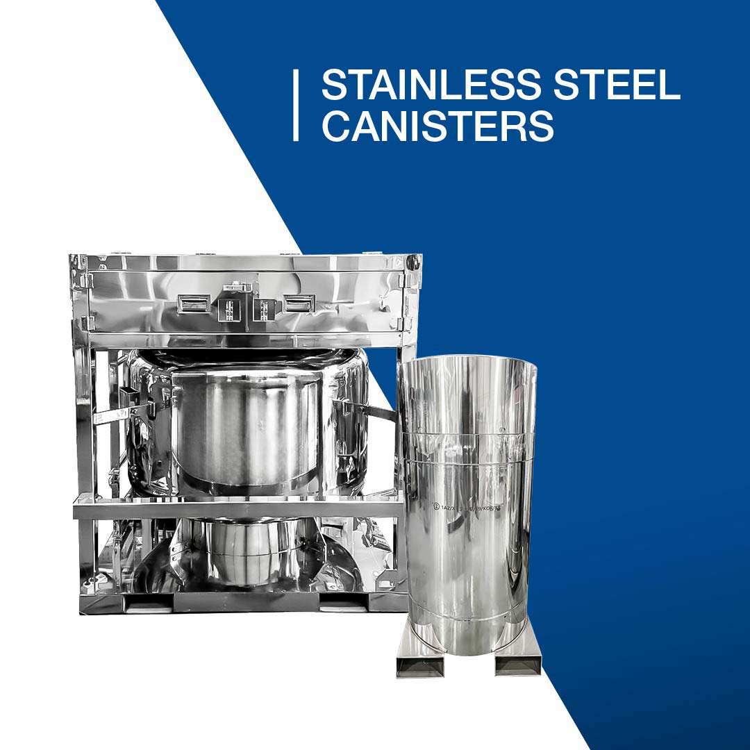
- Stainless steel canisters
- UHP gas valves,UHP pressure regulators and UHP fittings for carrier gases
- UHP gas valves, regulators and fittings for precursor gases
- Diaphragm valves, UHP gas pressure regulators and UHP fittings for SiH₄, NH₃
- N₂ purges between ALD sequences
7. Ion implantation
Ion implantation is the process of doping semiconductors by bombarding the wafer with ionized dopant atoms at high energy. This introduces controlled amounts of impurities (like boron for p-type or phosphorus/arsenic for n-type) into selected regions to modulate the silicon’s electrical properties.
Doping ions (B, P, As) are accelerated and injected into the silicon. This modifies the material's electrical properties and forms the transistor's active zones. The gases used are toxic and sensitive.
The dopant sources for ion implantation often come in gas form, especially for high currents. Common implant gases include arsine (AsH₃) for arsenic, phosphine (PH₃) for phosphorus, boron trifluoride (BF₃) for boron, and sometimes decaborane (B₁₀H₁₄) for boron or other tailored molecules. These gases are extremely hazardous (AsH₃ and PH₃ are highly toxic; BF₃ is corrosive and toxic), and they must be ultra-high purity to avoid introducing other impurities during implant.
Our key solutions for ion implantation:
- Vaccum integrated Valves integrated Pressure Regulators
- Controllers, diaphragm valves, pressure regulators and fittings for PH₃, BF₃, AsH₃
- Safety systems with automatic purging and double containment
8. Annealing
After ion implantation (and at various other points), wafers undergo annealing – heating to high temperatures for short durations – to repair crystal damage and activate dopant atoms electrically. Annealing is also used for other purposes, like dopant drive-in diffusion, silicide formation, or film property modification.
This step briefly heats the wafer (up to 1050°C) to repair crystalline defects and activate dopants. It uses controlled atmospheres of N₂, Ar or forming gas (N₂ + H₂).
Our key solutions for annealing:
- Diaphragm valves, pressure regulators, fittings and MFCs for N₂, Ar, forming gas
- Safety purge systems and UHP stainless steel valves
9. CMP (planarization)
CMP is a process used to planarize (flatten) the wafer surface by abrasive polishing combined with chemical etching. As multiple layers build up during fabrication, CMP is essential to achieve a flat surface before lithography of each layer (especially for interconnect layers and shallow trench isolation).
The wafer is mechanically and chemically polished to flatten its surface. This enables subsequent layers to be deposited uniformly. Post-CMP drying is a critical point.
Our key solutions for planarization:
- UHP diaphragm valves, pressure regulators and fittings for UHP N₂ used in streak-free drying process
10. Cleaning (wet/dry cleans)
Cleaning steps are interwoven throughout fabrication to remove contaminants, particles, or residues from previous processes. Wafers are repeatedly cleaned to ensure that each layer is deposited or patterned on a pristine surface.
The wafers are cleaned several times: with chemical baths (HF, SC1, SC2) or plasma (O₂, H₂, SF₆). The aim: to remove particles, residues, metals. Each rinsing and drying process requires absolute purity.
Our key solutions for cleaning:
- Distribution panels of UHP N₂ for flushing/drying processes
- Pressure regulators, valves, and fittings for UHP O₂ systems for plasma ash
Conclusion
From initial oxidation to final cleaning, every stage of semiconductor manufacturing relies on ultra-pure gases and distribution equipment. Our solutions ensure performance, safety and reliability, meeting the growing demands of the industry.


